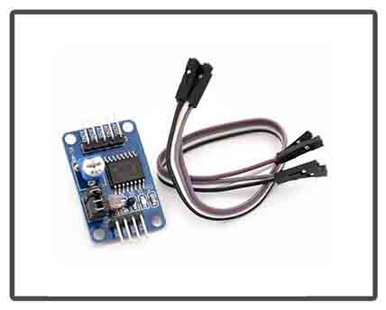
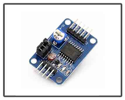
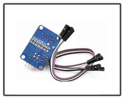
PCF8591 AD/DA Analog-Digital-Analog Converter Module Description Key indicators: Single-Supply Operation PCF8591 operating voltage range of 2.5V to 6V Low standby current through the I2C bus serial input / output PCF8591 by 3 hardware address pins addressing Sampling rate PCF8591 I2C bus rate decided 4 analog inputs programmable as single-ended or differential inputs Automatic incremental channel selection PCF8591 analog voltage range from VSS to VDD PCF8591 built-in track and hold circuit 8-bit successive approximation A / D converter through an analog output DAC gain Discription: 1. A module chip using PCF8951 2. module supports external voltage input capture (input voltage range 0-5v) 3. Three modules integrated photoresistor acquisition environment through the AD intensity accurate numerical 4. modules integrated thermistor, can capture the precise value of the ambient temperature through the AD 5. The five-module integrated 1 channel 0-5V voltage input acquisition (blue potentiometer to adjust the input voltage) 6. modules with power indicator light (on the module after power indicator lights) 7. modules with the DA output indicator light board DA output indicator module DA output interface voltage reaches a certain value, the voltage the greater the light brightness is more obvious; 8. module PCB size: 3.6cm * 2.3cm 9. standard double-sided, plate thickness 1.6mm, the layout is nice, surrounded by the through-hole, aperture: 3mm, convenient fixed Interface: The module's left and right, respectively, the external expansion of 2-way pin interface, respectively, as follows: Output interface of the left the AOUT chip DA The AINO chip analog input interface. AIN1 chip analog input interface AIN2 chip analog input interface AIN3 chip analog input interface The right side of the SCL IIC clock interface to access the microcontroller IO port The SDA IIC digital interface connected microcontroller IO port GND module to an external VCC power supply interface external 3.3v-5v Module red jumper instructions for use Module three red short circuit cap, respectively, the role are as follows: P4 connected to the P4 jumper, select thermistor access circuit P5 connected to P5 jumper to select the photoresistor access circuit P6 connected to the P6 jumper, to select 0-5V adjustable voltage access circuit Polybag
ˇˇ